
SEM Lab
Our SEM lab is for examining structures on the nano-scale, and analysing the elemental content using the EDX.
For access to the lab, or for any general training, please contact the lab leader, Dr Yang Li, or their deputy Dr Wing Chung Liu, For training on any of the equipment, please contact the Principal User or their deputy for the listed equipment.
All equipment in the SEM Lab needs to be booked before use. The booking system can be found here.
SEM – EDX Model: Magellan 400 SEM equipped with a load-lock, an in-lens and a back-scatter secondary electron detectors (normal imaging), Bruker X-ray detector (elemental analysis), stage bias (imaging dielectric samples), two CCDs for sample navigation and stage side view. A mini sputter-coater is available in the SEM lab to pre-coat SEM specimens with a conducting layer (Al, Au and C targets are available). This tool is to be used ONLY in conjunction with the SEM work. Users in Charge: Leader: Dr Yang Li Deputy: Dr Wing Chung Liu | 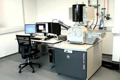 |
Sputter Coater Model: Quick and easy way to sputter-deposit conducting layers of Al, Au and C onto samples before SEM. This tool is to be used ONLY in conjunction with SEM work. Users in Charge: Leader: Dr Yang Li Deputy: Dr Wing Chung Liu | 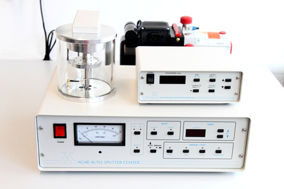 |
Quantum Design (Loaned to the CGC) FusionScope (AFM in SEM) The unique FusionScope Cantilever Technology is based on self-sensing cantilevers that allow for high-quality, low-noise detection of surface properties. The cantilevers are equipped with a full piezo-resistive Wheatstone bridge that provides all cantilever signals electrically without the need for optical alignment. This has direct advantages for the performance and ease of use, letting users record better images with less effort. The self-sensing technology also allows maximum access for the electron beam to the cantilever and sample region and enables a seamless combination of AFM and SEM. These self-sensing cantilevers are available with a broad variety of resonance frequencies, spring-constants and tip functionalities which provide the right cantilever for every application. For advanced measurement modes, specialised cantilever tips are used that enable, among other measurements: electrical conductivity, magnetisation, surface potentials, temperature, and other sample features. Users in Charge: Leader: Mr Sohail Abbas Deputy: Dr Wing Chun Liu | 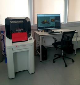 |
Wire BonderModel: HB16 Wedge, ball and ribbon bonding making use of Gold, Aluminium, Silver and Copper wires can be performed as using this facility either in manual or automatic mode Users in Charge: Leader: Dr Yang Li Deputy: Dr Wing Chung Liu | 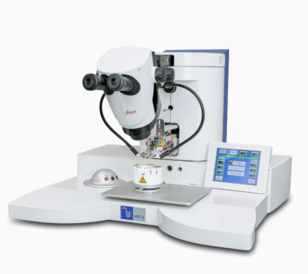 |
Solar SimulatorModel: Sol3A Class AAA Solar Simulators A Solar Simulator is a light source that approximates the illumination of natural sunlight. Solar simulators with various tailored spectral output are used to to test a variety of samples including but not limited to solar cells, sun screen (SPF), materials photo-stability, and other samples (in-vivo or in-vitro) under controlled, repeatable, laboratory conditions. Users in Charge: Leader: Sohail Abbas Deputy: Dr Wenshuo Xu | 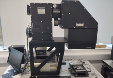 |
Quantum Efficiency Measurement SystemModel: The "quantum efficiency" (Q.E.) is the ratio of the number of carriers collected by the solar cell to the number of photons of a given energy incident on the solar cell. This system is designed to achieve the measurement. Users in Charge: Leader: Sohail Abbas Deputy: Dr Wenshuo Xu | 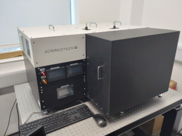 |
When in the SEM laboratory, please follow the local rules, downloadable here.