
CGC Class 100 Cleanroom
Below, you can find the list of equipment available in Class 100 cleanroom. A few are already available for use, others are being installed and will become available later.
Please use the booking system to use the equipment.
Electron-Beam Lithography (Royce EBL Suite)
A state-of-the-art high-resolution/throughput electron-beam lithography system capable of exposing 8-inch wafers. Principal User: Dr Yang Li Deputy User: Mr Petros Symeon | 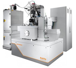 |
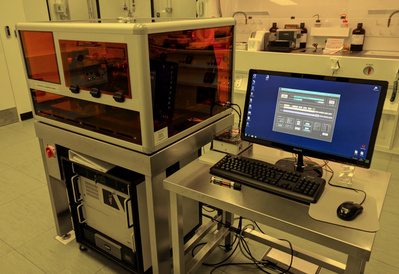
Laser WriterPrincipal User: Mr Petros Symeon Deputy User: Mr Sohail Abbas Model: LW-405B+, Microtech Srl
|  |
NanoimprinterModel: Obducat Eitre 6 with UV curing option Principal User: Mr Sohail Abbas Deputy User: Dr Dharmaraj Periyanagounder The tool is used for high-resolution nanoimprinting. | 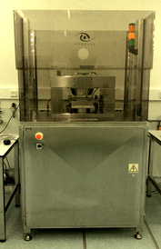 |
Resist Preparation Wet BenchThe wet bench is equipped with three spinners and four precision hotplates from EMS. Processes available: - SU-8 negative photo-resists - AZ/LOR positive and negative photo-resists - PMMA/ZEP e-beam resists Principal User: Dr Dharmaraj Periyanagounder Deputy User: Ms Lu Chen | 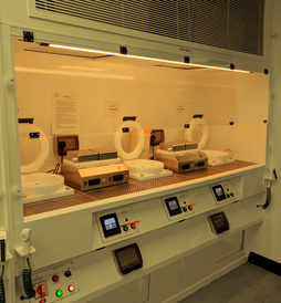 |
Development and Cleaning Wet BenchThis wet bench is used for preparation of samples for lithography, as well post-processing (development, etc.). Principal User: Dr Dharmaraj Periyanagounder Deputy User: Ms Lu Chen | 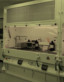 |
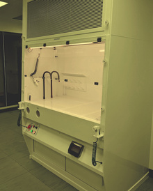
Acid Wet BenchLeader: Dr Dharmaraj Periyanagounder Deputy: Ms Lu Chen
|  |
Triple FurnaceThe tool is used for the deep oxidation of Si.
|
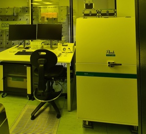
Park AFM NX20Principal User: Dr Yang Li Deputy User: Mr Sohail Abbas AFM Mode:
The Park AFM NX20 is a high-resolution atomic force microscope (AFM) designed for precise nanoscale imaging and analysis. It features advanced non-contact mode technology, automated operation and low-noise performance, making it ideal for materials science, nanotechnology and life sciences research. Sample size: Up to 200 mm (8 inches).
| 
|

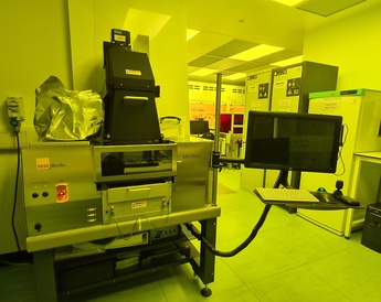
SUSS Mask and Bond Aligner MA/BA8 GEN4Principal User: Dr Yang Li Deputy User: Mr Petros Symeon The MA/BA Gen4 MA/BA8 delivers exceptional process results through its advanced automation. Features such as constant dose mode, an automated exposure time control unit and auto-alignment optimise process parameters for enhanced precision. Equipped with the high-performance MO Exposure Optics system, it ensures ideal exposure conditions for superior outcomes. Additionally, its sophisticated mechanical design enhances adjustment accuracy, with a specially engineered top- and bottom-side microscope unit (TSA and BSA) that minimises TSA microscope travel and reduces vibrations for improved stability. Our system is equipped with the TSA option. Wafer size: 1'', 2'', 4'', 6'', 8''.
|  |
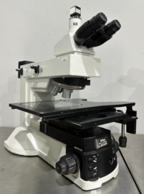
Inspection Microscope Nikon EclipseMotorised Sample Scanning Stage (Microscope)Model: Nikon Eclipse TE200 Microscope The Nikon Eclipse TE200 is a high-quality inverted fluorescence microscope, ideal for live cell imaging and tissue culture applications. Featuring Nikon’s advanced CFI60 optics, it delivers excellent image clarity and supports multiple observation modes, including brightfield, phase contrast and fluorescence. The TE200 is user-friendly, compatible with digital imaging systems and widely used for cell biology and advanced research in modern laboratories. Users in Charge: Leader: Dr. Yang Li
|  |
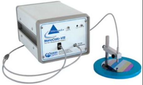
NanoCalc ReflectometerThis thin film reflectometry system analyses optical layer thickness from 10 nm to ~250 µm and allows for single thickness observation with a 0.1 nm resolution. This system is ideal for in situ, online thickness measurements and in removal rate applications. It can also measure the thickness of oxides, SiNx, photoresist and other semiconductor process films. It also measures anti-reflection coatings, anti-scratch coatings and rough layers on substrates such as steel, aluminium, brass, copper, ceramics and plastics. Thin film characteristics are typically measured through spectral reflectance/transmission and ellipsometry. The NanoCalc Thin Film Reflectometry System uses the reflectance method and measures the light reflected from a thin film over a wide range of wavelengths, with the incident light normal to the sample surface. Users in Charge: Leader: Mr Sohail Abbas
|  |