Our Atomic-Force Microscopy Lab is for examining structures on the atomic scale.
For access to the lab, or for any general training, please contact the lab leader Dr Yang Li, or their deputy Sohail Abbas. For training on any of the equipment, please contact the Principal User or their deputy for the listed equipment.
All equipment needs to be booked before use. The booking system can be found here.
|
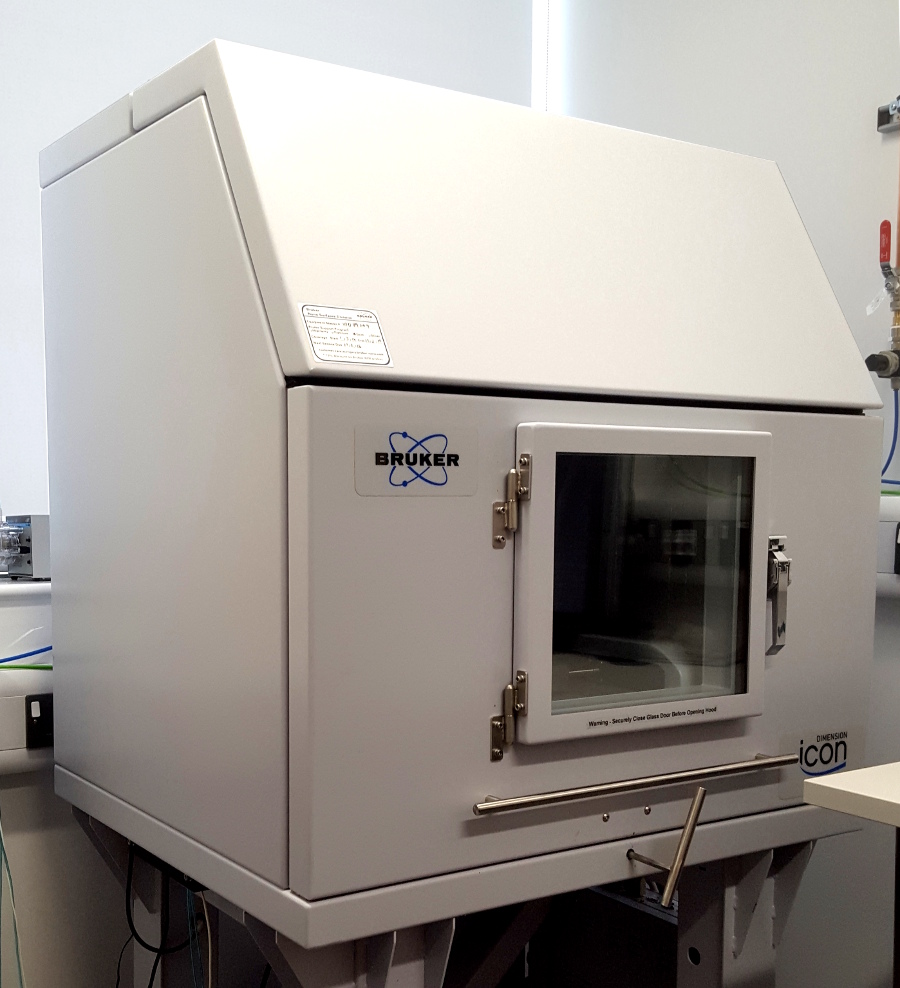
Atomic Force Microscope (AFM)
Model: Bruker Icon
Used for surface characterisation of samples.
Capabilities:
1. Topography modes:
• PeakForce Tapping (with ScanAsyst)
• Tapping mode
• Phase Imaging
• Contact mode
2. Electrical modes
• PeakForce Tunnelling AFM (PFTUNA)
• Kelvin Probe Force Microscopy (KPFM)
• Scanning Capacitance Microscopy (SCM)
• Electric Force Microscopy (EFM)
• Scanning Tunnelling Microscopy (STM)
3. Magnetic Force Microscopy (MFM)
4. PeakForce Quantitative Nanomechanical Mapping (PFQNM)
5. Lateral Force Microscopy
6. Microscope Image Registration & Overlay option (MIRO)
7. Heating/Cooling Temperature Controller (–35 ℃ to 250 ℃)
Users in Charge:
Leader: Dr Yang Li
Deputy 1: Sohail Abbas
Deputy 2:Dr Hamideh Ramezani
|
|
|
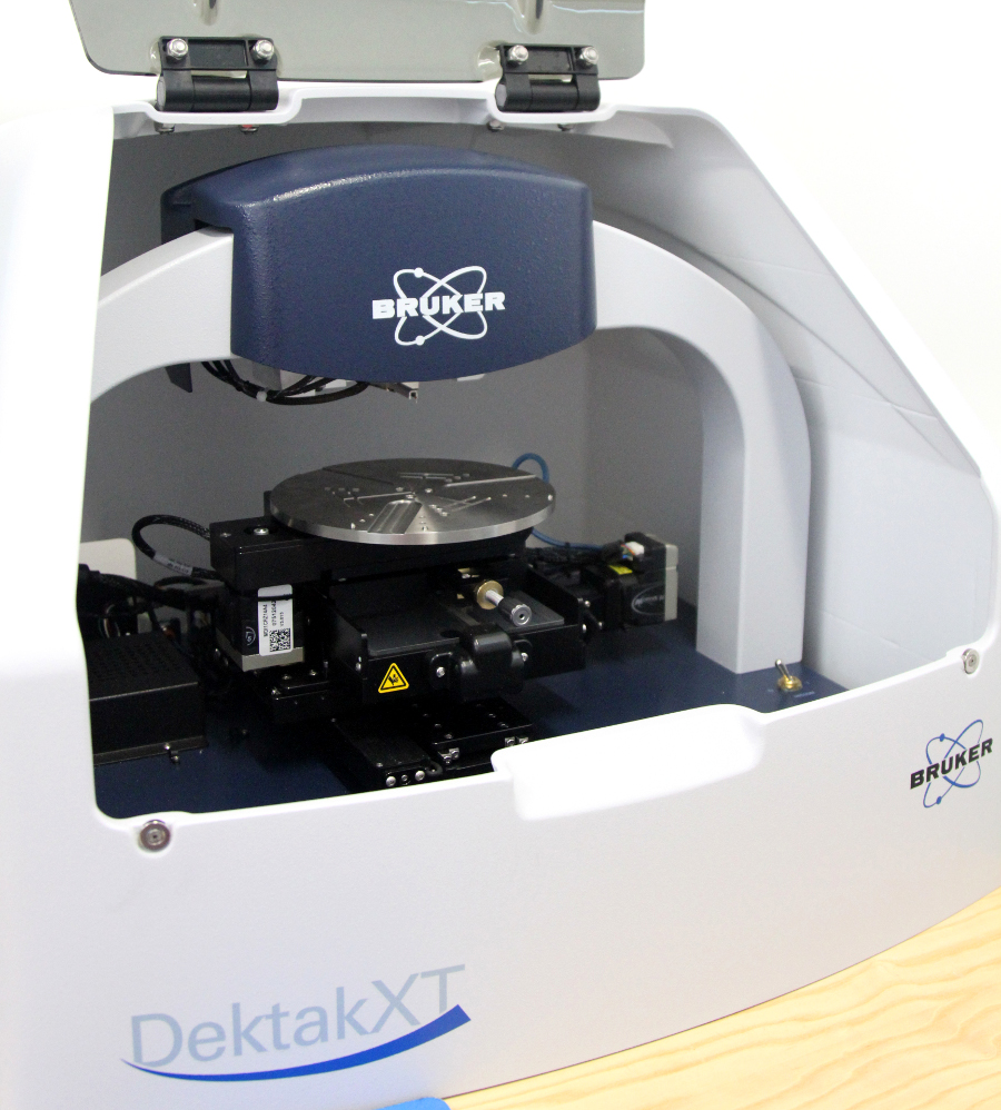
Profilometer
Model: Bruker Dektak XT Stylus
Used for thickness/step measurements and 3D mapping.
Capabilities:
1. Line scans
2. 3D Mapping
3. Wafer sized samples
4. Scan length between 50 µm and 55,000 µm (55 mm) for a non-stitched measurement
5. Stitching capability for scan length of 55mm to 200mm
6. User-programmable stylus force from 1 mg to 15 mg
7. Z resolution:
• 6.5 µm range provides a vertical bit resolution of 0.1 nm.
• For general applications, the 1.0 nm vertical resolution of the 65.5 µm range is usually adequate.
• When measuring thick films or very rough or curved samples, select the 524 µm range with 8.0 nm resolution.
Users in Charge:
Leader: Dr Yang Li
Deputy: Sohail Abbas
Deputy:Dr Hamideh Ramezani
|
|
When in the AFM laboratory, please follow the local rules, downloadable here.
Photos by Samuel Curtis Photography


